Zettl Research GroupCondensed Matter Physics |
|||
 |
November 2019MXenes are two-dimensional (2D) transition metal carbides or nitrides produced by etching of the aluminum or silicon from a bulk MAX phase (M=transition metal, A= Group 13 or 14 element, X= C, N). This etching process imparts a negative surface charge on the nanosheets, allowing aqueous or organic inks that are amenable to a variety of printing processes. MXenes also show high electrical and thermal conductivity, making these materials attractive for electrochemical and energy storage applications. By combining the MXene sheets with a surfactant, it is possible to stabilize the particles at liquid-liquid interfaces through a jamming effect, where the liquids can be kinetically-trapped in non-equilibrium shapes. In this work, the jamming effect has been exploited to 3D print arbitrary designs of MXene inks in an organic solvent. The reconfigurable nature of this entirely liquid system allows on demand formation of complex constructs with potential applications in electronic, electromagnetic and electrochemical devices. Sculpting liquids with two-dimensional materials: The Assembly of Ti3C2Tx MXene Sheets at Liquid–Liquid Interfaces | |
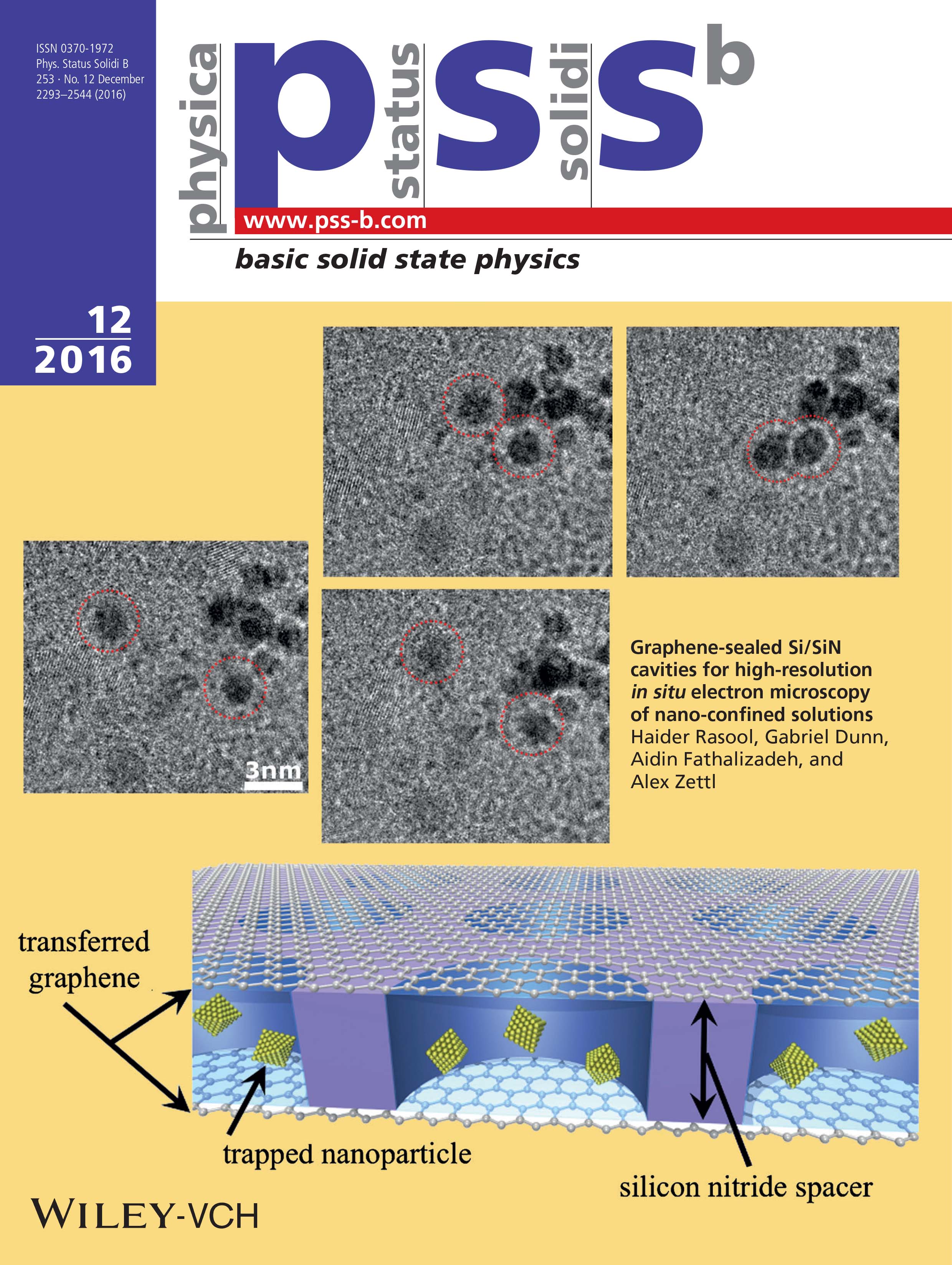 |
January 2017We demonstrate new liquid cell architectures utilizing graphene-sealed Si or SiN cavities for in situ electron microscopy. While previous graphene liquid cell techniques have shown graphene to be an ideal sealing layer and electron-transparent viewing window, they trap irregular geometries of liquid with unknown sample volumes. Our new technique allows for a leak-proof confinement of liquids of precise volume in the tens of attoliter range while maintaining the benefits of graphene as a viewing window. The utility of this new cell architecture is demonstrated by imaging the dynamics of gold nanoparticles in three dimensions with atomic resolution under a transmission electron microscope. Graphene-sealed Si/SiN cavities for high-resolution in situ electron microscopy of nano-confined solutions |
|
 |
January 2017"High resolution imaging in the graphene liquid cell," Chapter 19 in Liquid Cell Electron Microscopy |
|
 |
January 2016Gate-controlled tuning of the charge carrier density in graphene devices provides new opportunities to control the behavior of molecular adsorbates. We have used scanning tunneling microscopy (STM) and spectroscopy (STS) to show how the vibronic electronic levels of 1,3,5-tris(2,2-dicyanovinyl)benzene molecules adsorbed onto a graphene/BN/SiO2 device can be tuned via application of a backgate voltage. The molecules are observed to electronically decouple from the graphene layer, giving rise to well-resolved vibronic states in dI/dV spectroscopy at the single-molecule level. Density functional theory (DFT) and many-body spectral function calculations show that these states arise from molecular orbitals coupled strongly to carbon–hydrogen rocking modes. Application of a back-gate voltage allows switching between different electronic states of the molecules for fixed sample bias. High Surface Area MoS2/Graphene Hybrid Aerogel for Ultrasensitive NO2 Detection |
|
 |
June 2014We demonstrate that a back-gated graphene device can be used to switch between two different electronic states of adsorbed organic molecules (the LUMO and the LUMO+1). The image shows the experimentally measured local density of states associated with the LUMO (blue-white) and the LUMO+1 (red-white) of a molecular layer on graphene, obtained using scanning tunneling microscopy. Image courtesy of Alexander Riss. Imaging and Tuning Molecular Levels at the Surface of a Gated Graphene Device |
|
 |
March 2011We report direct mapping of the grains and grain boundaries (GBs) of large-area monolayer polycrystalline graphene sheets, at large (several micrometer) and single-atom length scales. Global grain and GB mapping is performed using electron diffraction in scanning transmission electron microscopy (STEM) or using dark-field imaging in conventional TEM. Additionally, we employ aberration-corrected TEM to extract direct images of the local atomic arrangements of graphene GBs, which reveal the alternating pentagon-heptagon structure along high-angle GBs. Our findings provide a readily adaptable tool for graphene GB studies. Grain Boundary Mapping in Polycrystalline Graphene |
|
 |
March 2009With a transmission electron aberration–corrected microscope capable of simultaneous atomic spatial resolution and 1-second temporal resolution, we produced movies of the dynamics of carbon atoms at the edge of a hole in a suspended, single atomic layer of graphene. The rearrangement of bonds and beam-induced ejection of carbon atoms are recorded as the hole grows. We investigated the mechanism of edge reconstruction and demonstrated the stability of the “zigzag” edge configuration. This study of an ideal low-dimensional interface, a hole in graphene, exhibits the complex behavior of atoms at a boundary. Graphene at the Edge: Stability and Dynamics |
|
|
|
July 2008Here we demonstrate a means to observe, by conventional TEM, even the smallest atoms and molecules: on a clean single-layer graphene membrane, adsorbates such as atomic hydrogen and carbon can be seen as if they were suspended in free space. We directly image such individual adatoms, along with carbon chains and vacancies, and investigate their dynamics in real time. Imaging and dynamics of light atoms and molecules on graphene. Other information, including TEM images of individual atoms, and movies of molecule dynamics, can be found here. |
|
 |
September 2008Here we demonstrate a room temperature, carbon-nanotube-based nanomechanical resonator with atomic mass resolution. ... Using this extreme mass sensitivity, we observe atomic mass shot noise, which is analogous to the electronic shot noise measured in many semiconductor experiments. Unlike traditional mass spectrometers, nanomechanical mass spectrometers do not require the potentially destructive ionization of the test sample, are more sensitive to large molecules, and could eventually be incorporated on a chip. An atomic-resolution nanomechanical mass sensor |
|
 |
November 2008We present a transmission electron microscopy investigation of graphene membranes, crystalline foils with a thickness of only 1 atom. By using aberration-correction in combination with a monochromator, 1-Ĺ resolution is achieved at an acceleration voltage of only 80 kV. ... We observe a highly crystalline lattice along with occasional point defects. The formation and annealing of Stone-Wales defects is observed in situ. Multiple five- and seven-membered rings appear exclusively in combinations that avoid dislocations and disclinations, in contrast to previous observations on highly curved (tube- or fullerene-like) graphene surfaces. Direct Imaging of Lattice Atoms and Topological Defects in Graphene Membranes |
|
 |
July 2007Gold nanoparticles have been self-assembled at the surface of both amine- and thiol-functionalized boron nitride nanotubes (BNNTs) in solution. ... This approach constitutes a basis for the preparation of highly functionalized BNNTs and their utilization as nanoscale templates for assembly and integration with other nanoscale materials. |
|
 |
February 2004Chemistry text cover used the Zettl Lab image of the spiral view of a nanotube. This image was also seen earlier on the cover of a Chemical and Engineering News issue in 1998 (see below). |
|
 |
October 2004Zettl Lab image was used on the cover of an IEEE special issue on Applications of Superconductivity. |
|
 |
February 2002Electron holography performed in situ inside a high resolution transmission electron microscope has been used to determine the magnitude and spatial distribution of the electric field surrounding individual field-emitting carbon nanotubes. The electric field (and hence the associated field emission current) is concentrated precisely at the tips of the nanotubes and not at other nanotube defects such as sidewall imperfections. The electric field magnitude and distribution are stable in time, even in cases where the nanotube field emission current exhibits extensive temporal fluctuations. |
|
 |
February 2001EYE ON THE FUTURE: NANOTECHNOLOGY hybrid NEMS By Paul Sharke, Associate Editor Molecular Motors Inching—er, nanometering—toward mechanical devices of an atomic scale, two researchers spell out practical considerations for MEs who will one day design them. Molecular Motors and Na-no Bearings and Engines: That's the way the agenda listed two speeches at ASME's recent nanotechnology workshop in Washington. For engineers in the audience inclined toward the pragmatic, surely these two talks, by Carlo Montemagno and Alex Zettl, would warrant attention. They did. |
|
 |
June 2000A Zettl Lab image was used on the cover of Physics World in a volume featuring a review of carbon nanotube research.
|
|
 |
June 1998The Zettl Research Group's image of a nanotube spiral featured on the cover of a Chemical & Engineering News volume highlighting materials to meet tomorrow's challenges. Note: the same image was featured on the cover of a Chemistry text in 2004 (see above). |
|
 |
November 1987A Zettl Lab image featured by the University of California at Berkeley's Alumni News magazine. |
![]()